In most of the time we need to step up, step down the DC voltage. In audio amplifier or DC motor control this DC to DC converter circuits will helps you. So in this article sharing a simple and high quality Step up and Step down converter using MC34063 circuit.
Key Features of This IC based Circuit
- Input voltage is 3V to 40V DC
- Few number of external components required for this circuit.
- Frequency operation to 100 kHz.
- Easy to assemble and you can build this in a small PCB.
MC34063 DC-DC converter control IC
The MC34063 IC is used for DC to DC conversion. The internal structure of this IC consist of temperature compensated reference, a comparator, controlled duty cycle oscillator with an active current limit circuit, a driver and a high current output switch.This IC based circuit can able to step-down, step-up and voltage inverting. The circuit need minimum number of external electronic components.
This IC can operate with an input voltage range from 3.0 V to 40 V and has a low standby current. This IC can capable of a high output switch current of up to 1.5 A and can operate at frequencies up to 100 kHz. The IC features a precision 2% reference and an adjustable output voltage.
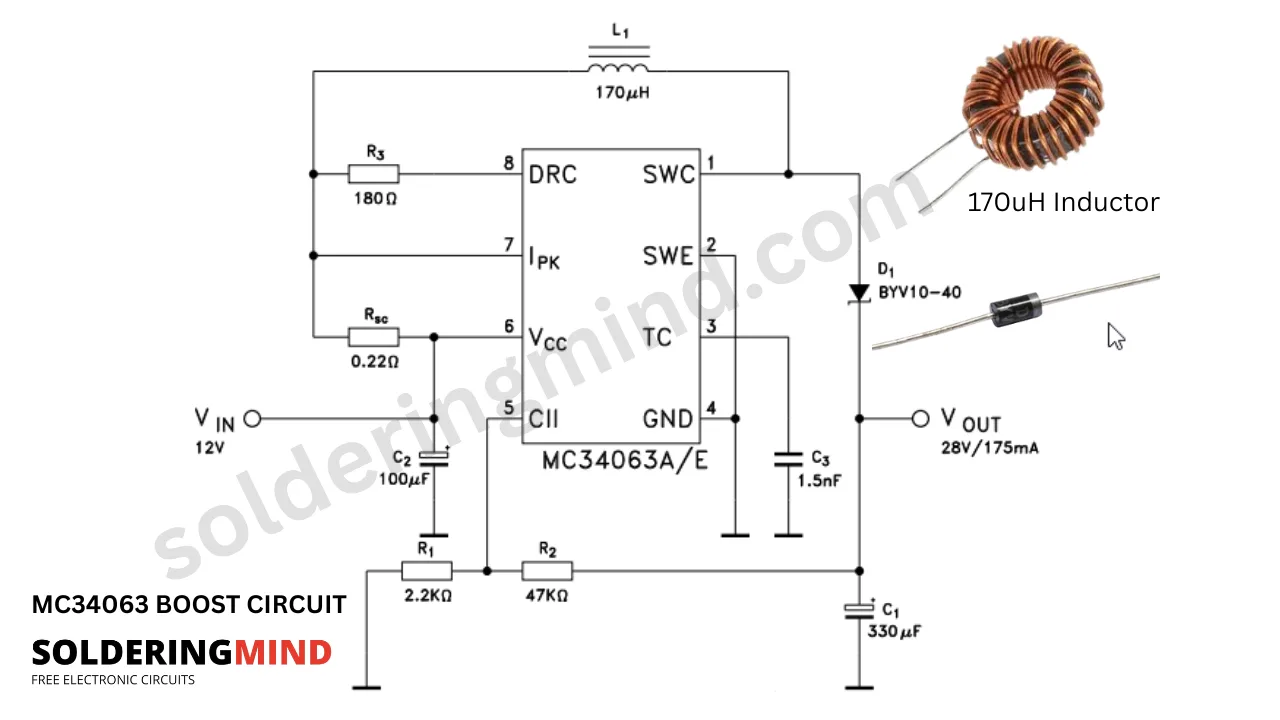
MC34063 Boost Circuit Schematic
The boost circuit will convert the low voltage input DC volt to high voltage DC. The given circuit diagram showing the input voltage of 12V DC is converted to 28V DC at 175 mA output. Boost circuit is useful for high voltage required circuits or electronic applications. The limitation of this circuit is its output current. if you are boosting the DC voltage then the output current will reduced.

Components Required
- MC34063 IC – The heart of the circuit (a switching regulator IC).
- L1 (170 µH Inductor) – Stores and transfers energy.
- D1 (BYV10-40 Schottky Diode) – Provides fast switching and low forward voltage drop.
- C1, C2, C3 (Capacitors) – For filtering, energy storage, and stability.
- R1, R2 (Voltage Divider) – Feedback resistors to set output voltage using the series connected resistor for stepdown voltage.
- Rsc (0.22Ω Resistor) – Current sense resistor (limits peak current).
- R3 (180Ω Resistor) – Part of the timing and internal transistor circuit.
Working Principle of Boost Converter Circuit
The MC34063 boost converter works on the principle of energy storage in an inductor and controlled switching. When the internal transistor of the IC is switched ON, current flows through the inductor (L1), causing it to store energy in its magnetic field.
During this period, the diode (D1) is reverse-biased, so no current flows to the output. When the switch turns OFF, the magnetic field in the inductor collapses, and the stored energy is released. This sudden release of energy adds to the input voltage, creating a higher voltage at the output, which is then passed through the diode to the capacitor (C1) for storage and filtering.
The IC MC34063 will regulates the output voltage by continuously comparing the portion of the output voltage (fed back through resistors R1 and R2) with its internal reference voltage. If the output drops below the set level, the IC will increases the duty cycle it means it keeps the switch ON for longer to boost the voltage. If the output voltage is rises too high, the IC reduces the duty cycle.
Meanwhile, the current sense resistor (Rsc) protects the circuit by limiting the maximum current through the inductor, preventing the damage to the IC and components. This cycle of charging and discharging the inductor repeats rapidly, producing a stable DC output higher than the input.