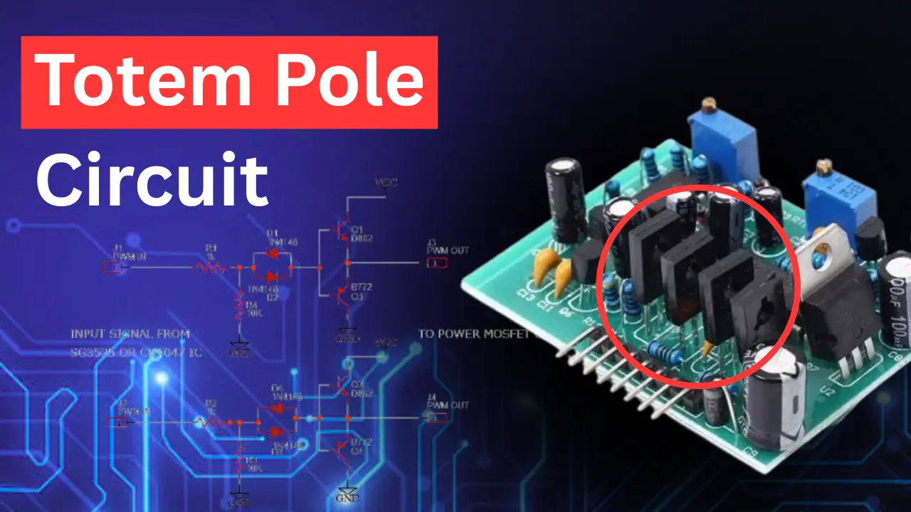
The Totem Pole Driver Circuit is commonly used to driving the gate pin of the power MOSFETs in switching applications such as in SMPS circuit, inverters and DC-DC converters. This circuit is using for the purpose of high current to quickly charge/discharge the gate pin of a MOSFET so it will improving the switching speed and it will has a low impedance push-pull output stage to drive the gate of the MOSFET effectively.
What is a Totem Pole Circuit?
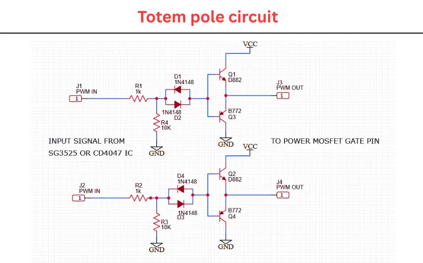
The totem pole circuit is a transistor based pre output stage circuit of inverter or SMPS. It driving or providing the high current to the gate pin of the connected MOSFET. So this circuit can easily turn on or off the output power transistors or MOSFETs. In the provided circuit diagram, the totem pole configuration is built with a pair of complementary bipolar junction transistors of D882 and B772 and it is stacked vertically, which will resembling a “totem pole.”
The transistors are controlled by a PWM signal from driver ICs like the SG3525 or CD4047. When the PWM signal is high, the NPN transistor turns ON and it will pulling the output to high current. This push pull action makes the fast switching of the connected MOSFET and it will reducing the switching losses and improving its overall efficiency.
Why is it Called a Totem Pole?
The term “Totem Pole” is comes from the visual resemblance of the entire circuit’s and transistor arrangement to a totem pole structure. where the components are stacked vertically one above the other. It will looks like carvings on a totem pole. In electronics, this refers to the stacked configuration of transistors and used to control an output node.
The given circuit the NPN transistor of D882 is sits on top position and it is connected to Vcc and the PNP transistor of B772 is at the bottom position it will connected to ground. This vertical arrangement allows the circuit to actively pull the output both high and low, so this will providing a strong push pull operation. This totem pole configuration is providing,
- Fast switching speeds
- Low output impedance
- Efficient gate driving capability
Circuit Diagram
Components Required
| Component | Value / Part Number | Quantity |
|---|---|---|
| R1, R2 | 1kΩ | 2 |
| R3, R4 | 10K | 2 |
| D1, D2, D3, D4 | 1N4148 | 4 |
| Q1, Q2 | D882 (NPN) | 2 |
| Q3, Q4 | B772 (PNP) | 2 |
| J1, J2 | – | 2 |
| J3, J4 | – | 2 |
| Power Supply | 12V (recommended) | 1 |
As an Amazon Associate, I earn from qualifying purchases.
D882 General-Purpose NPN Transistors (Pack Of 10)
- Transistor Type: NPN
- Max Collector Current(IC): 3A
- Max Collector-Emitter Voltage (VCE): 30V
- Max Collector-Base Voltage (VCB): 40V
- Max Emitter-Base Voltage (VEBO): 5V
As an Amazon Associate, I earn from qualifying purchases.
10Pcs B772 PNP Medium Power Transistor
- Transistor Type: PNP
- Max Collector Current(IC): -3A
- Max Collector-Emitter Voltage (VCE): -30V
- Max Collector-Base Voltage (VCB): -40V
- Max Emitter-Base Voltage (VEBO): -5V
Working Principle of Totem Pole Configuration
This totem pole driver circuit consist of 2 pars of transistor configuration which will push pull the signals to output with high current. This will gives a fast switching and efficient control of the connected load such as a MOSFET gate in power electronics.
- The transistor Q1 and Q2 are NPN transistors of D882 they will act as the high side switch.
- The Transistor Q3 and Q4 are PNP transistors of B772 which will acts as the low side switch.
- Diodes (1N4148) and resistors form the base drive circuitry to control these transistors.
- When the input PWM signal is high the NPN transistor turns will ON and pulling the output (PWM OUT) to high. When the PWM signal is low, this time the PNP transistor will turns ON and pulling the output low.
Applications of Totem Pole Circuits
- MOSFET and IGBT Gate Drivers.
- Push-Pull Output Stages.
- Audio Amplifier Driver Circuits.
- Inverter circuit.