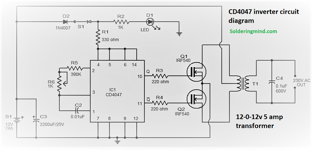
CD4047be 100w inverter circuit diagram with PCB layout – The inverter circuit is working based on the oscillating ic of CD4047. It is a general-purpose inverter ic you will get in all the electronic shops. This simple inverter circuit can deliver 100 watts power output with 220v ac.
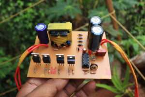
100 watt inverter circuit cd4047
The inverter is an electronic device that converts the dc voltage to ac voltage wit the help of Step-up transformers. The inverter is essential in a time of electricity failure or load shutdown of the power in your house.
- Also check SG3525 ic inverter circuit and PCB layout
This homemade inverter circuit will provide the same frequency and voltage needes for your electrical equipment. The output frequency and the current is:-
- 220v ac with 100 w at (50hz)
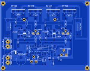
CD4047 inverter PCB
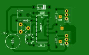
Connect the positive voltage on the +12v place. and the negative connection is in the MOSFETs area. TR1 and TR2 are the connection for the transformer. use 12-0-12 5 amp transformer to get 100w power output.
Inverter power calculator
The power is based on the voltage and the ampere of the supply. so the power is defined as the multiplication of voltage and the current.
Power ( watts ) = Volt ( v ) * current ( A )
so, power = 12v * 5A = 100w
Using 12-0-12 5 ampere transformer will gives upto 100 watts output.
CD4047 pinout
The ic 4047 is a CMOS low power monostable or astable multivibrator chip. the pin configuration of this ic is:-
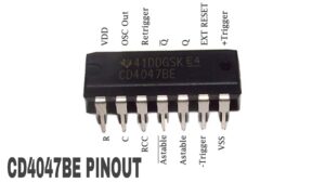
| PIN NUMBER | DESCRIPTION |
| 1 | c – used to connect the external capacitor |
| 2 | R- used to connect the external resistor |
| 3 | rcc – common pin for connecting thr capacitor and resistor to it |
| 4 | AST” – pin goes low when used astable mode |
| 5 | AST – goes high when using astable mode |
| 6 | – trigger – using in monostable mode we giving high to low inputs |
| 7 | Vss – negative pin of the ic |
| 8 | + trigger – on monostable mode gives low to high input |
| 9 | EXT reset – is an external reset pin |
| 10 | Q – giving normal out put signals for driving mosfets |
| 11 | Q’ – this is the second pin giving the signals for driving the mosfets |
| 12 | REtrigger – retriggering pin |
| 13 | OSC out – giving oscillated output |
| 14 | The positive pin of this ic |
Circuit Diagram