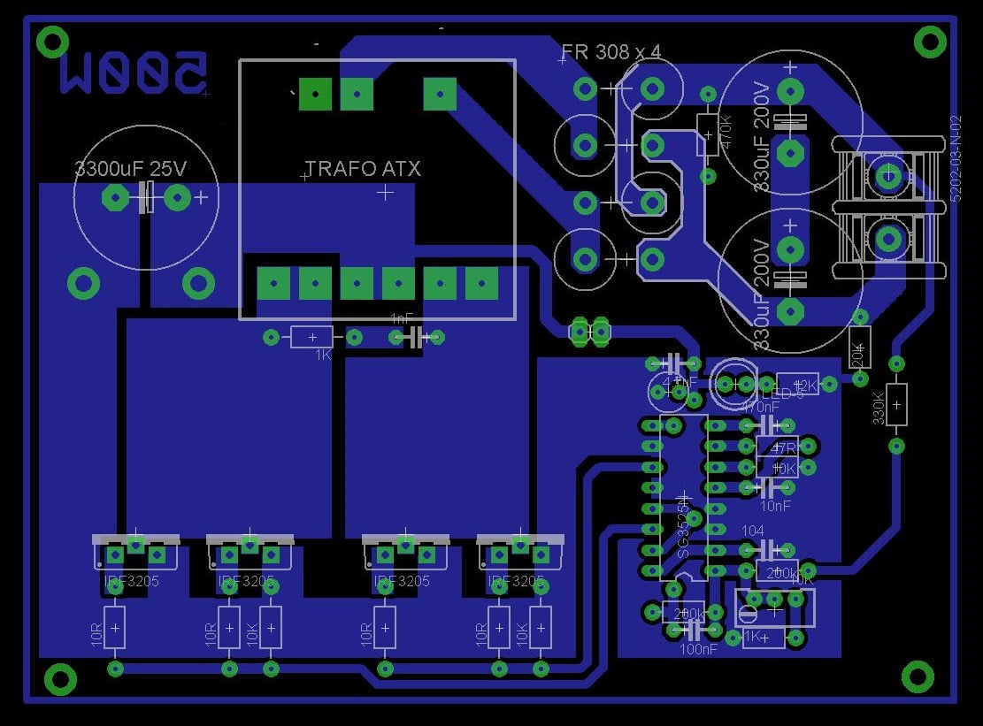
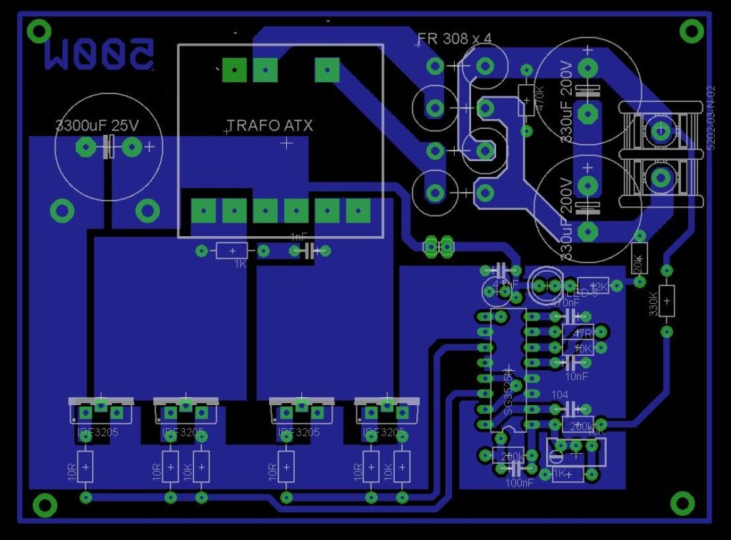
in this article, I’m going to explain the 500-watt dc to an ac inverter circuit and PCB layout. this is a simple and power inverter based on ATEX transformer ( you can get this from old SMPS of the computer ). the main advantage of this circuit is the size, the very small-sized inverter can provide up to 1000 watts ( maximum peak watts ). Check the inverter making video here
High Frequency Inverter PCB Layout Diagram
using this power inverter you can run drilling machines, mobile charger, mixi, ( recommended to not use electronic devices because it producing high frequency )
Components Required
- SG3525 ic ———————1
- ei33 transformer ( rewinded ) ——1
- 3300 uf capacitor——–1
- 330uf 200v capacitor——–2
- Irf3205 mosfet —–4
- 1k resistor—– 2
- 200k resistor ——- 2
- 330k resistor———1
- 104pf———2
- 10k preset pot ( bed type )—–1
- 4.7 uf 63v capacitor——1
- 10k resistor ——–2
- 10nf capacitor——-1
- 470 nf capacitor——1
Transformer used in the circuit
The transformer used is from ATEX. EI33 transformer and I rewinded the transformer ( the video of rewinding is available on my youtube channel. The primary coil of 3 + 3 turns and 90 turns on the secondary coil.
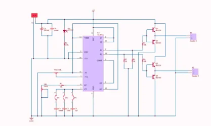
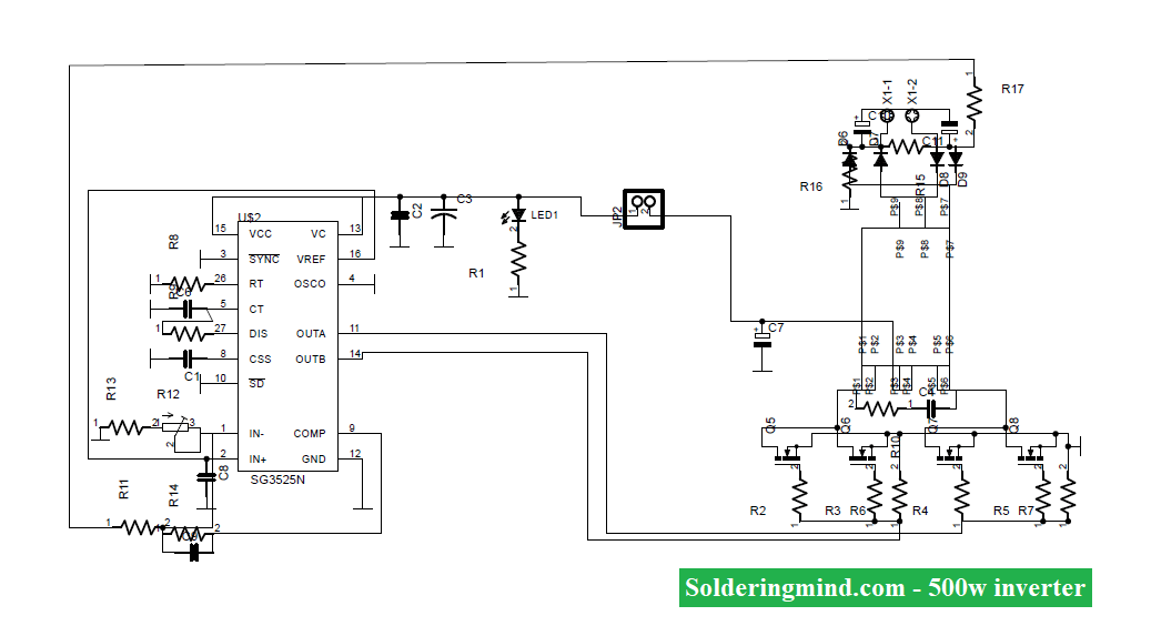
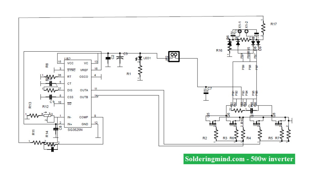
500 watts inverter circuit diagram
Working
the inverter is a High-frequency inverter that means the inverter circuit produces about 20-50 kHz frequency. so we need o use the atex transformer to get the output. the atex transformer is a high-frequency transformer it will only working on high-frequency input signals. the high frequency produced by the SG3525 ic and the signal can be amplified by the four IRF3205 MOSFETs. Use a minimum of 12 v 8-ampere transformer.
Caution: this circuit only designed for educational purpose any kind of illegal activities i am not responsible. and this circuit produces high voltage power supply so be careful when doing testing.