In audio power amplifiers, the DC voltage at the speaker output is an unwanted and that will damages the connected speakers permanently. Ideally, the amplifier output should only contain the AC audio signal. if a fault is occurs in the amplifier such as a failed transistor or coupling capacitor may result in a DC offset at the output.
To protect the speakers and amplifier a DC detection circuit is used. This circuit senses the presence of DC voltage at the amplifier output and generates a control signal to disconnect the speakers through a relay protection circuit.
Amplifier Output DC Detection Circuit Diagram
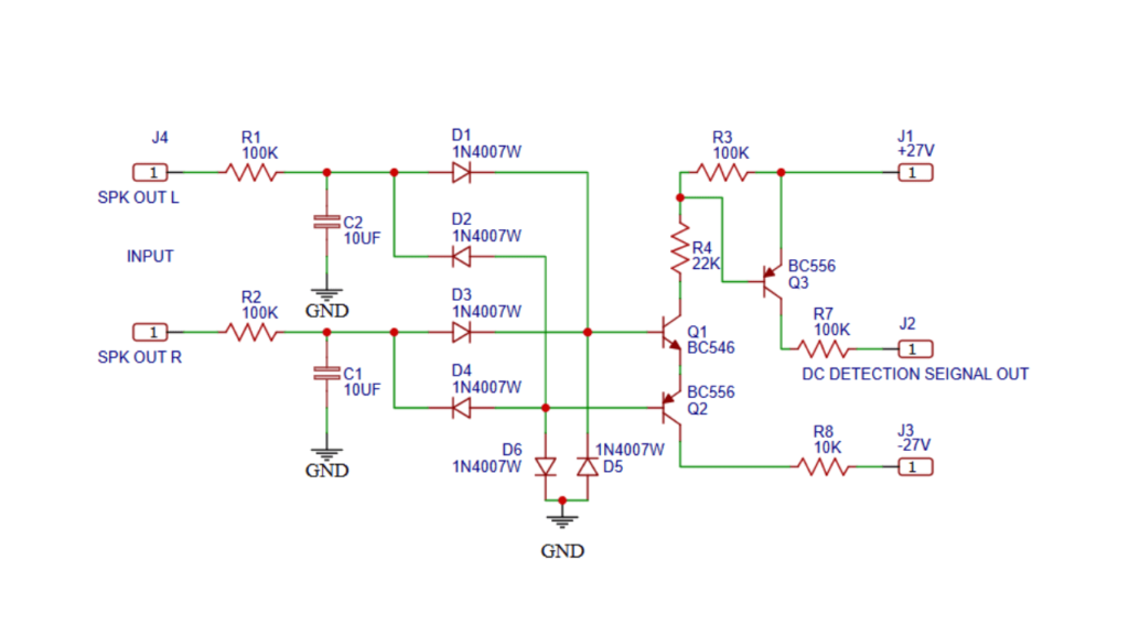
The given circuit monitors both left (SPK OUT L) and right (SPK OUT R) amplifier outputs. It combines their signals through resistors and diodes, and if any DC is detected, the transistors activate to produce a “DC Detection Signal Out” which can be used to trigger speaker protection.
Components Required
- R1, R2 (100kΩ): Input resistors that isolate the amplifier outputs.
- C1, C2 (10µF): Filter capacitors to remove normal AC audio signals.
- D1–D6 (1N4007): Diode network for DC level rectification and protection.
- Q1 (BC546): NPN transistor used for initial DC sensing.
- Q2, Q3 (BC556): PNP transistors that form part of the signal amplification and output stage.
- R3- 100k
- R8- 10k
- J1 (+27V) & J3 (-27V): Dual power supply inputs.
- J2: DC detection signal output.
Working Principle
The circuit continuously monitors the left and right speaker outputs from the amplifier through resistors R1 and R2. Under normal operating conditions, the amplifier output consists of an AC audio signal centered around 0V. The capacitors C1 and C2 filter out this AC signal, preventing it from triggering the detection stage. As a result, no significant voltage appears across the diode network, and the transistors remain inactive.
When a DC voltage appears at either speaker output, due to amplifier faults such as a shorted transistor or capacitor failure, it passes through the input resistors and is rectified by the diode network (D1–D4). The rectified DC voltage biases the transistor Q1 (BC546), which then begins to conduct. This conduction activates the following transistor pair Q2 and Q3, creating a chain reaction that amplifies the detection signal.
Once Q3 conducts, it generates a voltage at the DC Detection Signal Output (J2). This output can be fed to a relay driver or protection circuit that disconnects the speakers from the amplifier to prevent damage. When the DC fault disappears, the circuit returns to its idle state, allowing normal operation. Thus, the circuit effectively provides real-time DC fault monitoring and protection for the amplifier’s output stage.
Advantages
- Protects expensive speakers from DC damage.
- Detects both positive and negative DC voltages.
- Simple and low cost design using common components.
- Can be easily integrated with relay based protection circuits.
Applications
- Audio power amplifiers for home theater and professional sound systems.
- Speaker protection modules.
- Fault detection circuits in high-power amplifiers.
- Amplifier maintenance and testing setups.