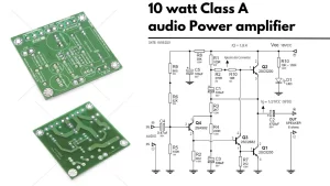
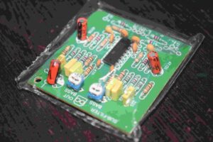
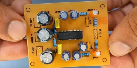
Friends, in this article, iam sharing the PCB layout and PCB layout files of Jean Hiraga Class A Amplifier Board. let’s build the famous Jean Hiraga Class A amplifier board. This amplifier produces an output power between 30 to 40 W RMS with a 30-0-30 V DC supply. You can use a 25-0-25 V 8A transformer.
Jean Hiraga Class A Amplifier Circuit Diagram
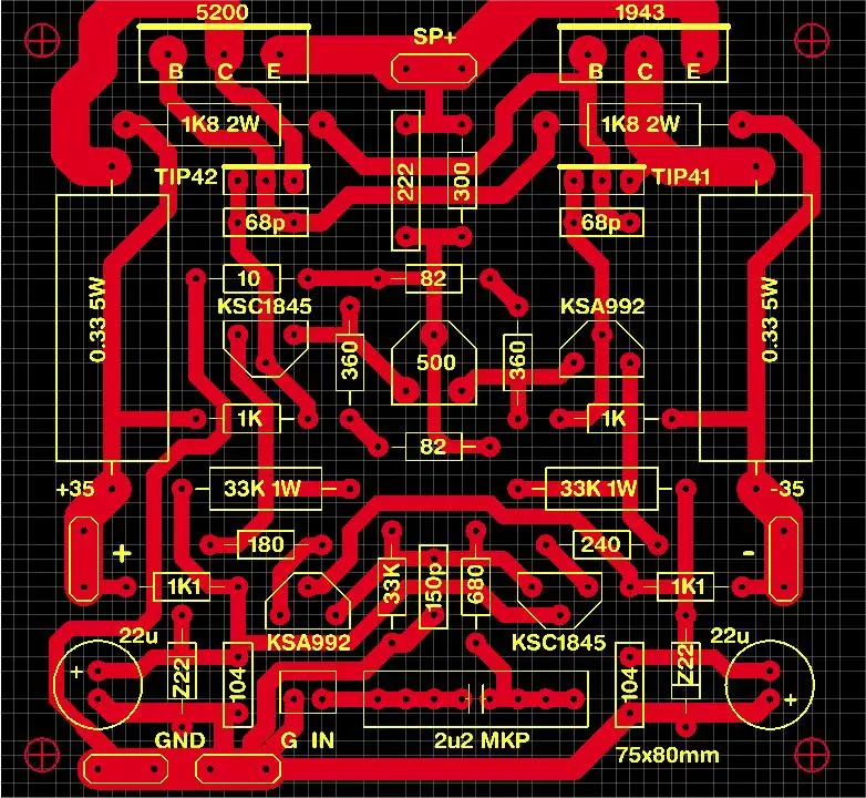
Circuit and Connection Explanation
The special value resistors used in this project were purchased from projectpoint.in, and the transistors were bought from etstore.in. The 500-ohm preset on the board is used to adjust the DC offset voltage. Keep the offset voltage at zero or as close to zero as possible. Wait for some time for the transistors to heat up, and then readjust if necessary.
The recommended bias current is 1 to 1.5 A. To measure the bias current, measure the voltage across the 0.33-ohm 5 W resistor and divide the voltage by the resistor value to calculate the current flowing through it. For example, in the video, I measured around 218 mV across the 0.33-ohm resistor. So, 218 ÷ 0.33 = 660 mA.
The bias current is controlled by the base resistor of the third and fourth transistors. In the video, I used 33k 1 W resistors and obtained a bias current of 660 mA. To get a 1 A bias current, use a 27k resistor. A 1 W resistor is used there mainly for better thermal stability. However, you can use a 0.25 W resistor if you do not have a 1 W type.
First, test the amplifier using a series lamp connected to the transformer primary and check that everything is working properly. While adjusting the bias and offset voltage, disconnect the series lamp and connect the transformer directly to the AC mains. Also, short the input and disconnect the speaker line during adjustment.
Class A amplifiers generate a lot of heat, so use a proper heatsink. The heatsink shown in the video is only for testing purposes. During testing, I attached larger heatsinks along with a cooling fan. Also, add heatsinks for the driver transistors of TIP41 and TIP42.