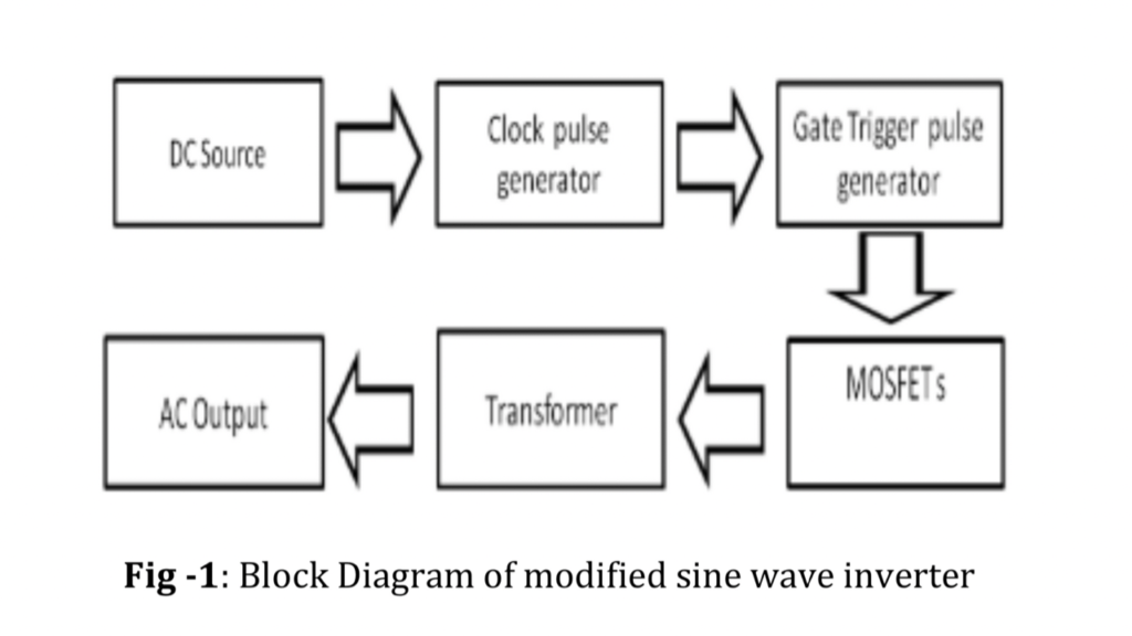
Inverter can be classified as square wave inverter, modified square wave inverter and also pure sine wave inverter. here i am introducing a modified sine wave inverter circuit diagram you can build at home easily. The CD4017 Inverter circuit diagram contains few components so the cost to build is very cheap.
Inverter Circuit Diagram

Components Required
| Component | Quantity |
| NE555 ic | 1 |
| CD4017 | 1 |
| 22K RESISTOR | 2 |
| 55N06 N CHANNEL MOSFET | 2 |
| LM7808 REGULATOR IC | 1 |
| 10UF CAPACITOR | 1 |
| 1NF | 2 |
| 0.1UF | 2 |
| 500K POT | 1 |
| 100K REISTOR | 1 |
| 100OHMS RESISTOR | 1 |
| 220 OHMS | 1 |
| 10-0-10V TRANSFORMER | 1 |
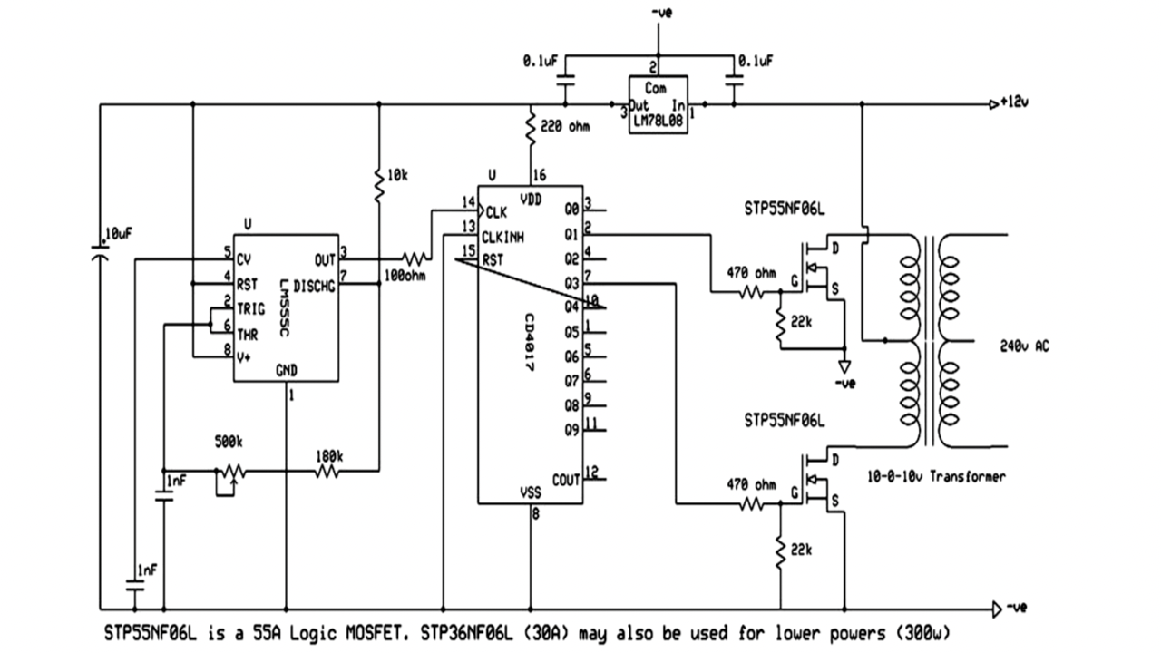
Modified Sine wave Using CD4017
Here 12V battery with the 7Ah capacity is using for this circuit. The CD4017 is a counter IC that giving the consecutive output from Q0 to Q9 when the clock pulse are available in the clock pin of the IC pin number 14.
The clock pulse giving by the 555 timer ic. The pinout of 3 from NE555 ic connected to the 14 th pin of CD4017 through a 100 ohms resistor. If we want 50 Hz output from the transformer then the timer output frequency must be equal to 4*50 = 200 Hz which can be created by adjusting the variable reistor of 50K.
STP55N06L Mosfet are using for 55A, 500 watt rating. In case of 30A and a low power rating Mosfet of STP36N06L is also using. Both the type of Mosfets are triggered from just 5V.