The TDA7293 is a monolithic integrated circuit in a MultiWatt15 package, intended for use as a high-performance audio power amplifier. It is a two-channel amplifier designed for use in hi-fi applications, and it can provide up to 100 watts of continuous average output power per channel into a 4-ohm load, or up to 68 watts per channel into an 8-ohm load.
The TDA7293 features thermal and short-circuit protection, as well as output impedance and load current diagnostic functions. It also has very low distortion and a wide range of voltage(40v-100v) and current capability. The TDA7293 also includes various features such as:-
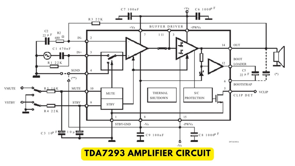
TDA7293 Amplifier Circuit Digram
- Differential Input Stage
- Internal Thermal Overload Protection
- Short Circuit Protection on the Output
- Muting Function
- The DC Servo
- Stand-by Function
- Diagnostic Output
It requires several external components to configure the amplifier correctly such as an input capacitor, DC blocking capacitor, feedback resistor, and coupling capacitor for the speaker.
Tda7293 IC Pinout
The TDA7293 is a multiwatt15 package, which has 15 pins. The pinout is as follows:
- GND: Ground connection
- VEE: Negative supply voltage
- IN-: Negative input of channel 1
- IN+: Positive input of channel 1
- VCC: Positive supply voltage
- OUT-: Negative output of channel 1
- OUT+: Positive output of channel 1
- GND: Ground connection
- VEE: Negative supply voltage
- IN-: Negative input of channel 2
- IN+: Positive input of channel 2
- VCC: Positive supply voltage
- OUT-: Negative output of channel 2
- OUT+: Positive output of channel 2
- ST-BY: Standby mode pin, active low
You should refer to the datasheet of TDA7293 for correct usages, such as absolute maximum ratings, recommended operating conditions, detailed electrical characteristics, and application circuit examples.
TDA7293 amplifier circuit. A typical TDA7293 circuit will require –
- Power supply (Vcc and GND)
- Input capacitors (Cin)
- DC blocking capacitor (Cdc)
- feedback resistor (Rf)
- Coupling capacitor (Cout)
- speaker load
Connection Details
- Vcc connects to pins 5 and 12
- Gnd connects to pins 1, 8 and 14
- Input signal connects to pins 3 and 10 (for channels 1 and 2 respectively)
- Cin connects between input pins and Gnd
- Cdc connects between the input pins and Vcc
- Rf connects between the input pins and output pins
- Cout connects between the output pins and the speaker
- the speaker connects to the output pins 6,7 and 13,14
- optional st-by pin is connected with a switch for on and off purpose
It’s worth noting that this is a basic diagram and the actual circuit will depend on the specific application and desired output, so you should always consult the datasheet from the manufacturer for recommended circuit diagrams and component values.