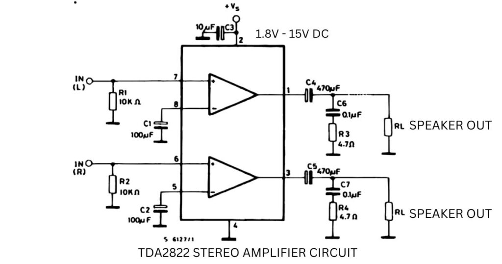
TDA2822 is a dual low-voltage power amplifier used in portable players or portable radio cassette players.
The main advantage of this audio amplifier is, that it works with a starting voltage of 1.8 to 15V DC supply. It can able to deliver an output wattage of 1.2 to 2 watt. This amplifier IC is most suitable for pre audio amplifier section because of low Crossover Distortion. The TDA2822 IC can be used to build stereo or bridge-mode audio amplifiers.
The IC package has two input and output terminals, it can easily deliver 250 milliwatts. The total package of integrated circuits is designed for low noise or distortion in the output speaker.
TDA2822 Amplifier circuit diagram
TDA2822 Pinout and Configuration
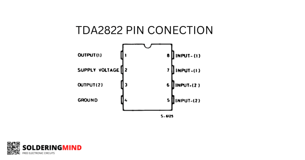
| PIN NUMBER | FUNCTION |
| 1 | Output 1 |
| 2 | Supply voltage (1.8 – 15V DC ) |
| 3 | Output 2 |
| 4 | Ground |
| 5 | – Input 2 |
| 6 | + Input 2 |
| 7 | + Input 1 |
| 8 | – Input 1 |
Components required
- TDA28822 / TDA2822M IC
- 10K, 4.7R Resistor
- 100uf/25v Capacitor
- 10uf, 470uf 25v Capacitor
- 0.1uf disc capacitor
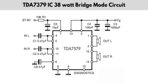
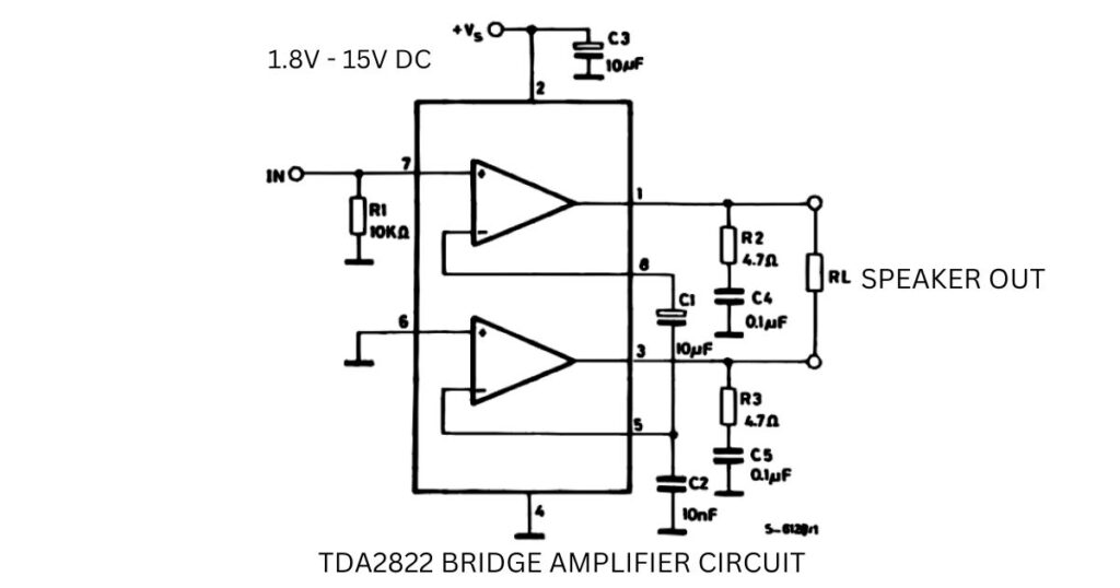
Bridge Mode Circuit diagram
Components required
- TDA2822/TDA2822m IC
- 10K, 4.7R Resistor
- 10NF, 0.1UF Capacitor
Also Check: 400 watt class D amplifier circuit and PCB layout