Green masking is a popular word because recently only the green color is used as the PCB masking. Nowadays blue, black color are also using for PCB masking. Why green masking of PCB needs? The green masking is important for protecting the copper tracks ( The circuit ) from contamination or electronics.
PCB – the printed circuit board. Which is masked with a green colour material is known as PCB green masking or masking ink of PCb.
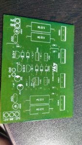
Understanding Green Masking of PCB
Green masking is a process of applying a masking coating upon the Printed circuit board to protect the circuit from oxidation and short circuit of the copper tracks. If you are not masked the PCB with coating material the copper-clad gets oxidizing and turns to green power. Then the copper track gets damage. So the coating material definitely have some specific properties that are given below
- Coating material should not remove by itself after applying on the PCB.
- It should be solder resist.
- Withstand with high temperature.
- Should contain transparency of copper track ( optional)
- If you are using screening method of printing the ink should be process the ease of cleaning.
Buy materials required for PCB soldermasking
- Silkscreen
- squeegee
- photo imageable or UV curable ink
- Photo emulsion
- Potassium dichromate
- Ferric chloride PURE FORM
Steps to do Green Masking on Printed circuit board
- Setup all required materials for PCB green masking. As mentioned above.
Steps
Taking printout of PCB layout and Soldering pad
In the first step, you need to take a printout of the PCB layout and the soldering pad design on butter paper. Notice: you need to take a negative image of the soldering pad as the pad is white and the surrounding space is black. Take the printout in a laser printer ( cartridge printing). Not the color jet printer. Cut the edges of the printout paper. And set aside for the next step.
Preparing Silk screen for screen printing
- Screen printing is the main method for applying the green masking on the printed circuit board. To prepare the perfect screen we need to do some things.
- The screen can buy from Here use this same high quality screen to get best print when you are doing.
- You need to make a design for screen printing first. We need to do an exposing method here.
- Take photocoat emulsions as per needed Quantity, and take a pinch of potassium dichromate ( sensitizer ) and dilute it with some drops of water.
- Mix the photocoat with pottasium dichromate vigorously in a dark room.
- Take the screen and wash it properly, apply the photo emulsion mixture on screen surface using squgee.
- Applying uniformly allover the surface of the screen.
- Important note: do this whole procedure in a dark room only do not allow to expose on the light.
- Dry the screen. Using dry air use power hair dryer for this ( do in dark room).
- After drying, the next step is to preparing the layout on screen.
Printing circuit using silkscreen
- The next step is to trace the circuit using the circuit ink
- place the appropriate size of the pcb under the silkscreen, then tight the screen and apply the circuit ink on the screen.
- spread over the screen first then, apply the pressure on squgee to apply the ink.
- after that take the PCB and dry it.
Etching PCB
- The the next step is very simple to understand. etching with ferric chloride solution.
- mix the small amount of ferric chloride anhydrous ( the pure form ) on water. mix well.
- allow to place the copper clad on it, shake vigorously.
- stop after whole unwanted copper has to be removed.
Applying Green coating on bottom of PCB
- This is the last step of PCB making, you need to arrange the screen with the soldering pad of the PCB and fix the screen very tight.
- Take a small amount of photoimagable ink or solder resistant ink and apply the half quantity of the hardener.
- mix well and adjust the thickness by using thinner.
- Apply the ink on screen and spread over the PCB. then takes the PCB and dry at high temperature. for 20minutes.
- next do a dip soldering , you are done