0-9 number generator circuit using CD4026 and NE555 IC. Hi friends welcome back with a random number picking circuit project using CD4026 and NE555 IC. This is a very interesting and hobby circuit for your home and college projects. You can use this projects for kids numbers prediction games, they will definitely enjoy this one. Also lot of project you can build with this basic circuit. So lets we begin.
CD4026 IC is a counter for a seven-segment display. It can drive a common cathode 7 segment display directly. The main feature of this IC is easy to interface with a timer or micron roller (TTL compatible). The IC can easily be cascaded with more IC to display the higher range of numbers in the display. The maximum clock frequency of this IC is 6 MHz. The package is available in PDIP, GDIP and PDSO packaging.
Circuit Diagram
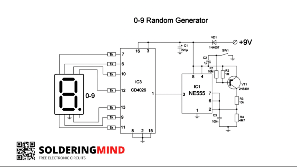
This circuit is based on a single seven-segment display. you can see the counting from 0-9. When you have pressed the button, then the circuit starts to generate the pulse from the timer IC. Then pick a random number from 0-9. This one is a funny project if you are interested in electronics you must feel the fun and the working principle of this.
The timer IC NE555 will produce the oscillated frequency and deliver through the PIN number 3 which will received by the display IC. The signal has to be injected in PIN number 1 of CD4026. When receiving the frequency that time the display IC starts to counting from 0 to 9. The oscillated signal will stops at a time then the display is also stop counting the numbers.
Components List
| PARTS | QUANTITY |
| LTS 543 common cathode 7 segment display | 1 |
| CD 4026 IC | 1 |
| NE555 IC | 1 |
| 2N5401 transistor | 1 |
| 1N4007 diode | 1 |
| 220uf/25v capacitor | 1 |
| 1uf/25v | 1 |
| 100nf (104PF) | 1 |
| Push switch | 1 |
| 10 M resistor | 1 |
| 1M | 1 |
| 10k | 1 |
| 4M7 | 1 |
| 1k | 7 |
| 9v battery | 1 |