Most of the mini audio systems is build with medium power audio IC like TDA2030 and LM1875 IC. the main reason for choosing this audio amplifier IC is cheap and suitable for home audio system. if you have old home theater box then try to open the box and you can able to see the amplifier board on it. It may contain the five pin IC it is a TDA2030 IC. Let’s’ look at the basics of TDA2030 along with its working and specifications.
What is TDA2030 IC?
The TDA2030 is a mini 5 pin IC, using as a low frequency class AB amplifier. It typically operates over a wide range of supply voltages. This IC is designed for the general purpose amplifier in audio applications, such as Hi-Fi systems and low power audio amplifiers.
With a few external components, it can deliver up to 14W of power into an 8 ohm load with a low harmonic distortion. The IC is the perfect choice for satellite amplifiers due to its simplicity, reliability, and cost effectiveness for audio amplifier designs.
TDA2030 IC Pinout
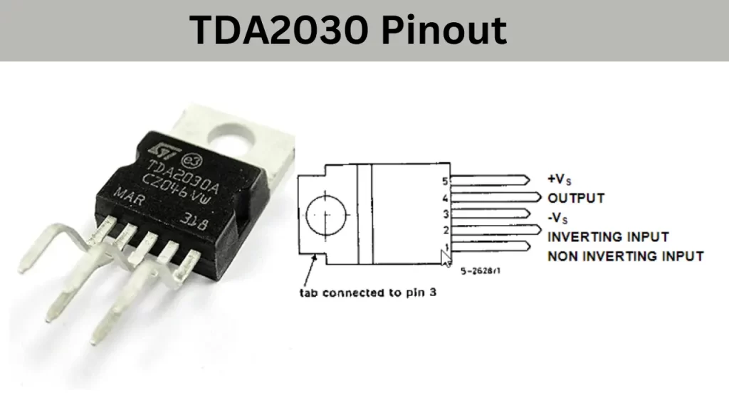
| Pin Number | Function |
|---|---|
| 1 | Non inverting input |
| 2 | Inverting Input |
| 3 | V- (power supply) |
| 4 | Output |
| 5 | V+ (Power Supply) |
Features of TDA2030 IC
- The IC can able to delivering the maximum output power of typically 14 watts into a 4 ohm load or 9 watts into an 8 ohm at ±14V power supply.
- The IC comes with low harmonic distortion and noise, this will makes it suitable for high fidelity audio applications.
- TDA2030 has a wide frequency response ranging from 20 Hz to 20 kHz, this is much more convenient for audio amplification across the audible spectrum.
- The input impedance of TDA2030 IC is very high, so it is compatible for any kind of audio input source.
- Low cost and minimal number of external components needs. This makes the circuit very small.
Working of TDA2030 as an Audio Amplifier
The TDa2030 is a low frequency Class AB audio amplifier IC. To know its working, you need to know the different stages.
- Input stage
- Voltage amplification stage
- output stage and feedback mechanism
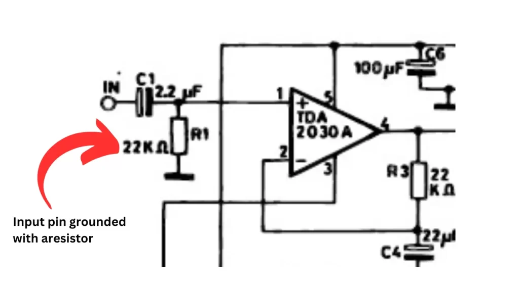
The Input stage the audio is fed here. This pin number of the IC is represented as Pin number 1 (The non inverting input). Most of the time a capacitor is using and the IC pin number 1 is grounded with 22K or 10K resistor to avoid humming sound in the audio amplifier.
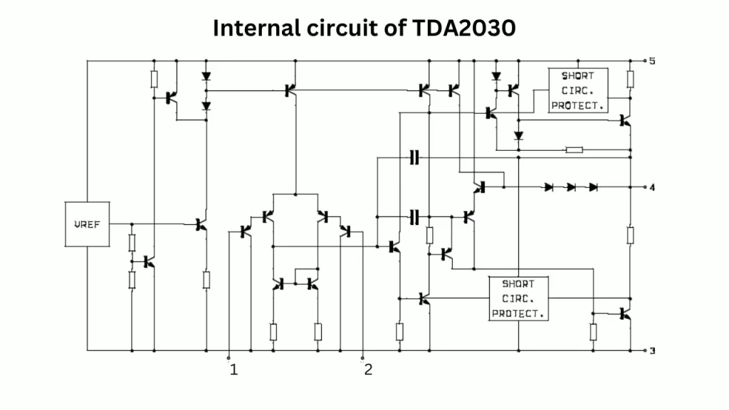
The next stage is Voltage amplification stage, here the input signal reach to the main audio amplification section and more number of push pull transistors amplify the audio signals. The internal circuit of TDA2030 is given below.
The final stage is Output stage, in this section the amplified signals get boosted. Additional current is added wit the output signals using internal power transistor. This output pin directly goes to the speaker input.
Application of TDA2030 IC
- Using for building Hi-fi audio amplifiers.
- Tda2030 works well with low frequency so it is suitable for subwoofer amplifier.
- Perfect choice for making stereo audio amplifier.
- Used in Car audio system and portable audio amplifier. Because of input voltage of 12v is required to work perfect.
Replacement for TDA2030
LM1875 and TDA2050 is the best suitable IC for replacement to TDA2030. Pin configuration are the same but the power rating and supply voltage and output watts are different. Comparing the cost wise the LM1875 is high cost than TDA2050.
TDA2030 14 watt Amplifier Circuit Diagram
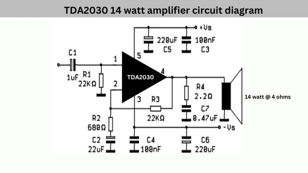
The 1uf electrolytic capacitor is connected directly to the pin 1 of the IC. This is the audio input pin, 22k resistor is also grounded to this pin to avoid input noise or disturbance from the input signal. 22k is connected with pin number 2 and 4 this is the feedback resistor. Two 220uf capacitor and 100nf capacitor connected in the input power supply to filter the AC pulse, which will gives the more filtered DC input. The pin number 4 is the audio output pin the 4 ohm speaker or woofer is connected with this pin and the other end in the ground connection. use high quality heatsink to avoid over heating of the IC.
FAQ
The TDA2030 is typically designed to operate within a specific voltage range to ensure proper performance and reliability. The maximum recommended supply voltage for the TDA2030 is typically around ±18 volts.
TDA2030 is a popular audio IC with the gain of 20 to 60dB.
The single TDA2050 IC can deliver upto 35 watts at 4 ohms speaker and 18 to 32 watts at 8 ohms speaker at 18 volt dual power supply.
TDA2050 is the better choice, because of high power output and simple circuit with few number of components.
It amplify the input audio signals and deliver upto 18 watts at 4 ohms speaker.