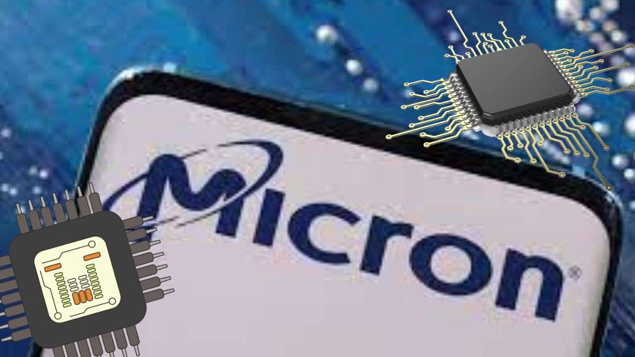

A leading memory chip company based in the United States has plans to establish a testing and packaging facility in Gujarat, India. The official announcement is expected to take place during Prime Minister Modi’s upcoming visit to the United States.
Officials from the Ministry of Electronics and Information Technology (MEITY) have informed that Micron Technology, a US-based memory chip company, has received approval from the Indian cabinet for its proposal to establish a semiconductor testing and packaging unit in Gujarat, India. The official announcement is expected to take place by Prime Minister Modi.
The ATMP (also known as OSAT – Outsourced Assembly & Test) plays a crucial role in the semiconductor world. Once wafers are created in wafer fabs or foundries, ATMP units cut them into chips, package, and test them for use in electronic products.
Independent semiconductor analyst Arun Mamphazy commented, “Right now, I’ll just say that having something is better than nothing, and we’re hopeful this will take off and succeed.”
Micron Technology choosing India for its testing and packaging unit is seen as a positive step towards India’s goal of becoming a semiconductor hub. While the government expected applications from major fabs like GlobalFoundries, Intel, TSMC, Samsung, and others, only three consortiums, including Vedanta’s, submitted semiconductor fab applications.”
The first round of applications, which began in January 2022, lasted only 45 days. On June 1 of this year, the government reopened the application window for the Modified Scheme for setting up of Compound Semiconductors/Silicon Photonics/Sensors Fab/Discrete Semiconductors Fab and Semiconductor ATMP/OSAT facilities in India. This opportunity will be expecting to available until December 2024.
Satya Gupta, President of the VLSI Society of India, shared with Business Today, “ATMP is an excellent way to kickstart semiconductor manufacturing in India. It requires relatively lower investment compared to wafer fabs, and the time to set up the factory is shorter. Depending on the complexity of the package type, investments can range from $30-40 million to $300-400 million. Most global experts suggest that India should start by building ATMP units before establishing larger wafer manufacturing plants. Additionally, unlike wafers, the output of ATMP units can be directly used by electronics product companies
