Making of PCB board at home is very easy. Most of them are things that I can’t make this kind of printed circuit board at home because they are very beautiful and they need big machines to cut, drill, and polishing of the board.
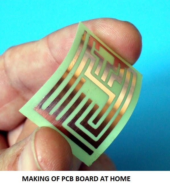
After reading this tutorial completely you will get ideas and better tutorials for how to make PCB at home. First, I want to tell you PCB printing is a very easy method, you don’t need to worry about it. I will help you to make the Electronic circuit board. PCB-making kits are also available in the online market.
Things you need for making PCB:
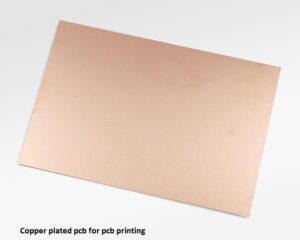
printed copper plate
Ferric chloride solution

Buy Ferric chloride for PCB etching it is available on Amazon or any nearest local electronics shops.
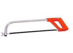
Cutting blade
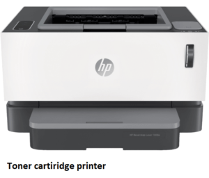
Laser printer (Toner cartridges)
Glossy paper

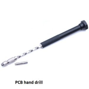
Hand PCB drill
Electric iron

Procedure for making PCB
- First, you must download the PCB layout (which circuit you have). example Download an Inverter circuit board PCB layout.
- Then open the PCB layout file, place the glossy paper in the laser toner printer, and click to print a copy of the PCB layout.
- Then take the printed page. Cut the layout using the printed board.
- Take the copper-plated board, and use a scrubber to remove the upper layer ( you feel the shining of the copper plate).
- Then cut the PCB as per the printed length of the PCB you want.
- Place the printed glossy paper upon the copper plate and iron it using an electric iron at a high temperature for 3 minutes.
- After ironing the PCB pour cold water and remove the paper. You will see the toner will be attached to the copper plate.
- Remove all the paper residues. then the clear path of connection becomes visible.
- Then pour some amount of ferric chloride powder into the water. mix well and slowly place the printed board into the Fecl 3 solutions.
- Gently shake this solution up to 5-10 min with uniformity.
- after removing the unwanted copper layer take it out from the solution and wash it.
- Dry the PCB board and remove the toner from the board by using the scrubber.
- Then place the component hole using a hand drill. then place the components and solder them.
- you are done



Thanks for sharing, Are you belongs to south India
You are always welcome